1 INTRODUCTION
The detector system is a key component to determine the scientific capabilities of space-and ground-based instruments. Therefore, the detailed understanding of the detector characteristics is required to develop astronomical instruments.
The charge-coupled device (CCD) was invented in 1969 in the AT&T Bell Labs by Willard Boyle and George E. Smith and has been used for scientific applications (Fossum 1993). Next-generation astronomical instrumentation will require the continuous improvement of the CCD performance to achieve a higher sensitivity and stability. Therefore, to precisely evaluate the characteristics of the CCD, a detector performance test system and its evaluation methodology are of great importance.
The photon transfer curve (PTC; plot of the relationship between signal and noise) is nowadays one of the most valuable techniques (Janesick et al. 1987) because it provides absolute information and concrete detector characteristics. This technique has been widely applied to various astronomical detectors to evaluate their performance. In addition, it can be applied to find the noise source in the system by comparing the results with the theoretical PTC results and to troubleshoot.
The Korea Astronomy and Space Science Institute (KASI) has been developing both ground- (Yuk et al. 2010; Oh et al. 2014) and space-based (Jeong et al. 2014) astronomical instrumentation. Recently, the Korea lunar exploration project has progressed to the development of a lunar probe and studies of the lunar mineralogy are planned (Lee et al. 2017; Kim et al. 2018). A well-equipped detector performance test system and accurate characterization are required for a successful scientific study. The KASI detector test system is equipped with a stable light source system that generates monochromatic light from 300 nm to 9 μm at a resolution of ~1 nm in the visible region; it includes flat illumination based on an integrating sphere. We evaluated the characteristics of the Andor iKon M CCD camera using this test system.
In the following sections of this paper, we present the detailed architecture of the KASI detector performance test system and the methods we used to measure the conversion gain, full well capacity, nonlinearity, dark current, read noise, pixel defects, and quantum efficiency. We also prove that the detector characteristics depend on the operating temperature. Finally, we compare our results with the test results of the vendor to verify and demonstrate that our measurement method and analysis are accurate.
2 KASI DETECTOR PERFORMANCE TEST SYSTEM
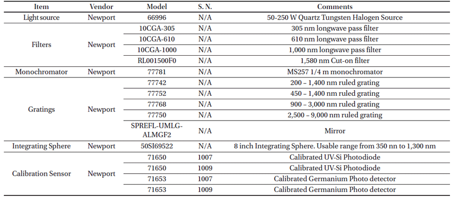
The goal of the KASI test equipment is to characterize variable detectors (from X-ray to IR) used for astronomical applications. The system consists of a light source, filter wheels, monochromator, integrating sphere, and two calibrated photo diodes (Fig. 1). The light source (Oriel’s 50–250 W Quartz Tungsten Halogen lamp) has a feedback system to regulate the input current for lamp stability and provide a continuous broadband spectrum from the visible to near-IR range (200–2,500 nm). It can be replaced with an IR radiation source for longer wavelengths. The integrating sphere has an 8” diameter. It is coated with barium sulfate and has three 2” ports. Its operating spectral range is 350 nm to 1.3 μm. It can be replaced by a gold-coated sphere for longer wavelengths. The filter wheel holds up to five 1” filters. Currently, it includes three longpass filters (305 ± 5 nm, 610 ± 5 nm, and 1,000 ± 5 nm) and one cut-on filter (1,580 nm), while one slot is open for white-light illumination of the detectors.
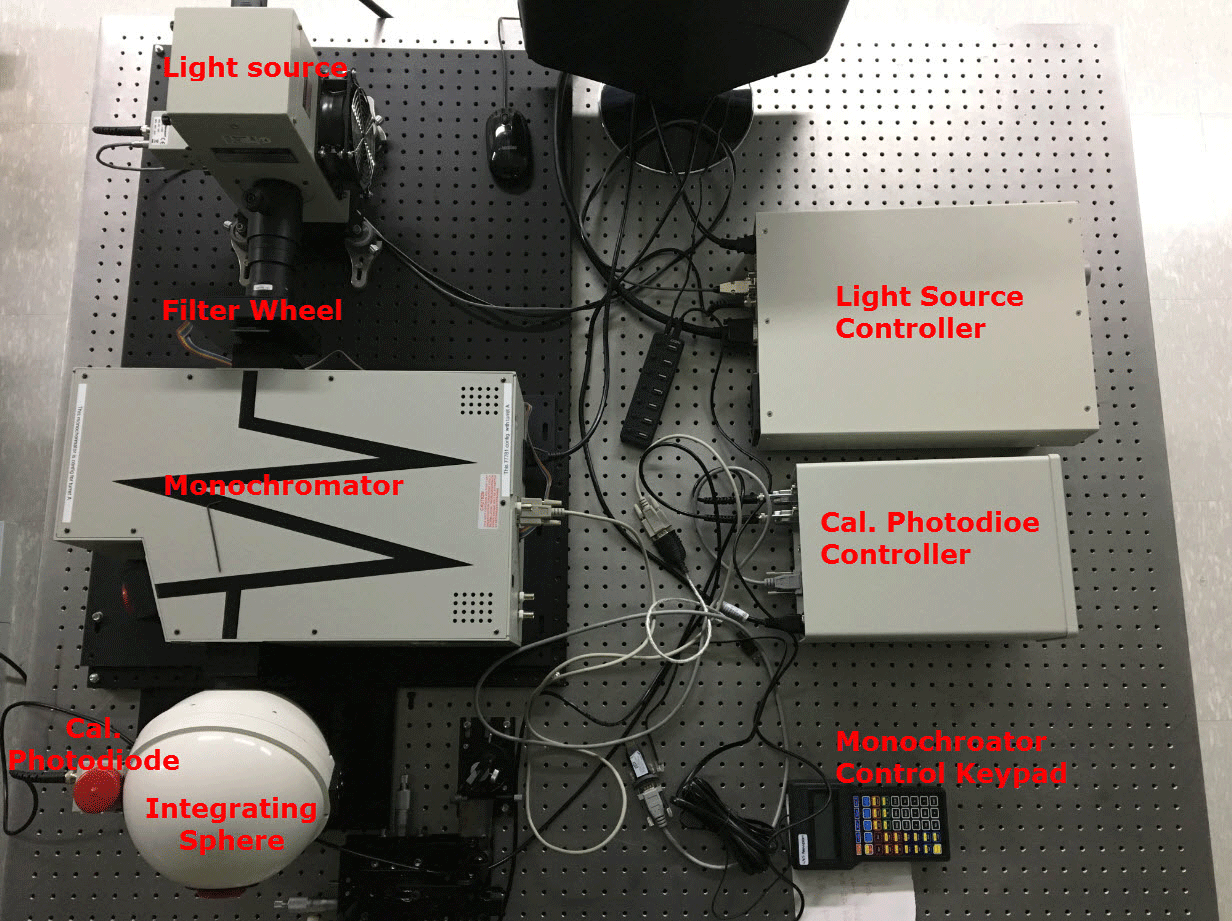
The Czerny–Turner monochromator consists of three diffraction gratings and one mirror. It can be operated from 200 to 9,000 nm depending on the selected gratings. One pair of UV silicon photodiodes and one pair of Germanium photo detectors has a 200–1,100 nm and 700–1,800 nm calibration range, respectively. In addition, a PbSe TE cooler will be used for the longer wavelengths (up to 5.5 μm) in the future. The main components of the KASI detector performance test system are summarized in Table 1.
3 CHARACTERIZATION OF THE ANDOR IKON-M CCD CAMERA
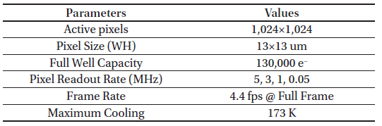
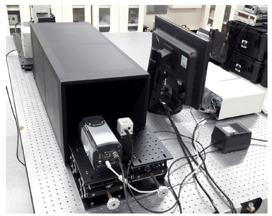
We characterized the Andor iKon-M (BEX2-DD) CCD camera. Its high sensitivity and low noise performance are ideal for astronomical applications. The detector is a full frame CCD with 1 K × 1 K pixel resolution and a 13 μm pixel size. The thinned backside-illuminated CCD produces a higher sensitivity and quantum efficiency than a conventional front-illuminated CCD. It is cooled down to an operating temperature of 173 K using a water cooler. Table 2 shows the specification summary for the Andor iKon M CCD camera (iKon-M 934 Series Specification, Andor). We set the vertical pixel shift speed to 4.25 μs and used a normal vertical clock voltage amplitude. In addition, the readout rate was 34 MHz at 16 bit and the preamplifier gain was 2X. Note that some of the characteristics, such as the nonlinearity and sensitivity, can be varied depending on the camera configuration. The camera setting and operation were managed using Solis (ver. 4.30), a software platform designed for image capture by Andor Technology and Python (ver. 3.5). The data analysis was carried out using Matlab (ver. 2017b). The characterization was performed in the KASI electronics laboratory (Fig. 2).
The CCD camera accumulates electrons generated from incident photons to analog voltage and converts them into a digital value. The electrical signal process therefore consists of many electrical conversion stages. The conversion gain, or system gain, represents the combination of gains in each stage and can be expressed as:
where Gpixel (e-/N) is the pixel gain, which indicates that the unit charge is converteed to the output voltage by the photodiode capacitance; GSF (V/V) is the gain of the source follower; GAMP (V/V) is the gain of the electrical stages based on the user-defgined gain setting; and GADC (V/ADU) is the gain of the conversion between analog voltage to digital units. To measure the conversion gain, Gtotal, procedures to measure each of the gains separately need to be developed. However, because the system conversion gain (Gtotal) itself needs to be measured, we used the PTC to induce the Gtotal.
Photon transfer was originally designed for test methodology for detector and camera systems; nowadays, it is applied for system level performance tests such as characterization, optimization, and troubleshooting (Janesick et al. 1987). An ideal PTC is divided into three distinct noise regimes. The first regime, read noise, represents random noise generated by the readout electrical circuit. Therefore, it should be measured without illumination. As the light illumination increases, the noise in the second regime, called “shot noise”, increases. The third regime is characterized by fixed pattern noise, showing a spatial pattern on the image. Among those three regimes, we used the characteristics of the shot noise to measure the conversion gain. Because shot noise follows a Poisson distribution, it is equivalent to the square root of the mean signal. Additionally, because the output signal in ADU is proportional to the accumulated electrons generated by incident photons, we can derive their relationship using Eq. (2).
where C.G represents the conversion gain (Gtotal), O represents the output signal in ADU, I represents the electrons generated by the incident photons and σ is the electron noise.
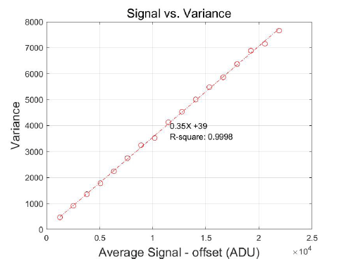
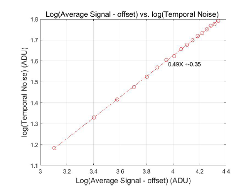
For the measurement of the conversion gain, we consecutively took two identical frames at the same exposure level until the images were fully saturated and then subtracted the first frame from the second on pixel by pixel. Subsequently, the subtracted image was divided by because random noise increases with the square root of the frame number. Finally, we plotted the results as function of the output signal (Fig. 3). Based on Eq.(2), the conversion gain is equal to the inverse of the slope in Fig. 3. Our measured conversion gain is 2.86 e-/ADU. In addition, we plotted the shot noise response as function of the signal on a log scale to verify the shot noise is correctly characterized using a slope of 0.5. Fig. 4 shows that the slope is very close to 0.5, which proves that the conversion gain was measured correctly.
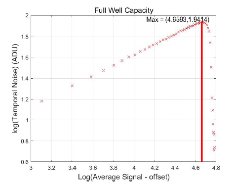
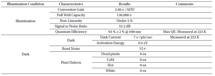
The full well capacity (FWC) defines the amount of the accumulated charge that an individual pixel can hold before saturation. Because it is affected by the number of manufacturing processes and operating conditions, such as the doping concentration and applied substrate voltages, individual pixels might have a slightly different FWC. Therefore, we exposed the detector to flat illumination by increasing the exposure time and calculated the FWC from the average output signal in the selected region (100×100 pixels in the middle of the images) of the plotted PTC. Because the noise in the shot noise regime is proportional to the output signal level (Fig. 5), the maximum level of noise represents the maximum output signal. Therefore, we multiplied the conversion gain with the maximum output signal to determine the FWC. The measured FWC is 130,000 e− and varies by ~1 %.
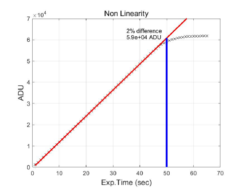
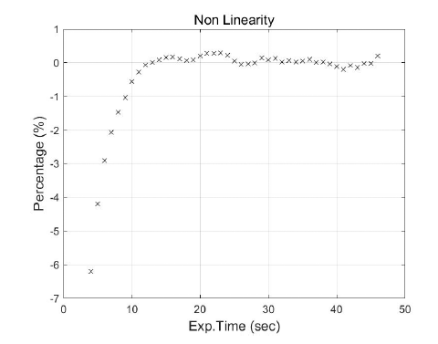
Nonlinearity is defined as the measurement of the camera gain as a function of the output signal levels. It is generally constant but varies at low and high signal levels. Good scientific detectors have a nonlinearity level within 2 % between 10 % and 90 % FWC. The measurements were performed by exposing the detector to flat illumination from the integrating sphere and selecting 100×100 pixels with increasing exposure time. Fig. 6 shows that nonlinearity greater than 2 % occurs above an FWC of 90 %. Fig. 7 shows that the nonlinearity is within 2 % between 10 % and 90 % FWC but deviates by 2 % more at low illumination.
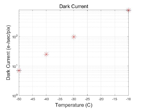
Because dark current is generated by thermally excited electrons, the temperature is a main contributor. A high level of dark current will limit the FWC and reduce the dynamic range of the detector. The analysis was performed by measuring the signal with increasing exposure time while the shutter was fully closed to isolate any external illumination. This procedure was repeated at different temperatures to determine the temperature dependency. In Fig. 8, the dark current is plotted versus the temperature. The lowest dark current is 7 e−/s/pix at 223 K and the dark current doubling temperature, which is the double dark current in temperature, is 5.3°C ± 0.2°C.
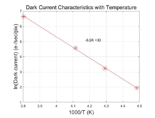
The dark current generation mechanism can be divided into three main components. First, the generation current is generated by an indirect transition in the depletion region of silicon (Sze 1985). Second, the diffusion current is generated by minority carrier approaches by diffusion process. Third, the surface generation current is generated by an abrupt discontinuity of the silicon lattice structure. Because the surface generation current can be suppressed by the manufacturing process, such as the inversion layer (Teranishi 1982), the two remaining components mainly generate dark currents. Widenhorn et al. (2002) divided the dark current components as function of the temperature. Because the characterization was performed above 223 K, the generation current is dominant and can be expressed as:
where ID is the dark current, k is the Boltzmann constant, T is the temperature, and ΔEg is the activation energy. Measured dark current data were modeled using Eq. (3) and an activation energy of 0.6 eV was determined (Fig. 9).
Read noise, called noise floor in PTC, is defined as randomly variable noise that comes from the readout electronics without any illumination. Read noise is a combination of a number of noise sources. Janesick (2007) expressed the read noise equation as shown in Eq. (4).
where SF represents the source follower noise, Reset represents the reset noise, Dark_Shot and Dark FPN repre-sent the dark current noise, ADC is the ADC quantizing noise, Off_FPN is the offset FPN, and System is the system noise.
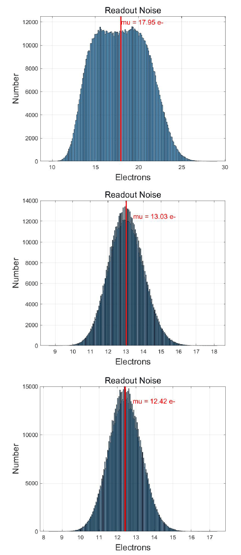
For the measurement, we obtained 100 consecutive images using the shortest exposure time (0.001 sec) and calculated the standard deviation of the pixel-to-pixel and mode values. However, because the read noise does not follow a Gaussian distribution at higher temperature, as shown in the top image in Fig. 10, we calculated the mean value instead of the mode value at this temperature. This is mainly due to the noise component, which is related to the dark current. It dramatically enlarges the pixel-to-pixel variation. The measured read noise is 18 e− at 263 K, 13 e− at 243 K, and 12.4 e− at 223 K (Fig. 10).
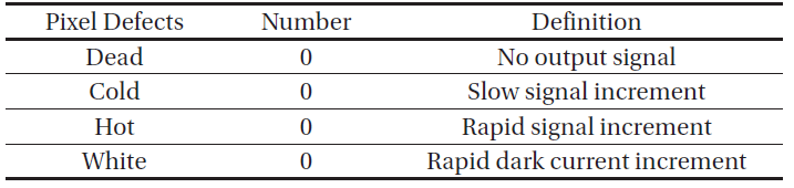
All individual detector pixels have different characteristics because they are affected by many manufacturing processes. Therefore, some pixels cannot respond appropriately to illumination. Those pixels are defined as pixel defects and they can be categorized into dead or black pixels, cold pixels, hot pixels, and white pixels. The positions of the defected pixels should be determined for the removal, masking, and/or correction of the data.
First, dead pixels cannot accumulate electrons with increasing illumination and have constant pixel values with or without illumination. Dead pixels are detected by determining if the pixel values increase or not with increasing exposure time. We did not detect any dead pixels. Second, cold pixels are defined as pixels with lower pixel values than that of the nearest neighbor pixels. We defined cold pixels as pixels with a value below 20 % or more than the median value of the surrounding neighbor pixels during mid–full well depth illumination and identified no cold pixels. Third, hot pixels are equal to cold pixels but have higher pixel values. No hot pixels were found. Fourth, white pixels are pixels that have a much higher dark current increment than that of the nearest neighbor pixels without illumination. We defined white pixels as pixels with a 20 times higher dark current increment than that of the surrounding neighbor pixels and found no white pixels. Table 3 shows the number of detected pixel defects. Finally, we investigated column defects, that is, several vertical or more contiguous defective pixels; but, no column defects were found.
The quantum efficiency (QE) is the ratio of the number of photo-generated charges to that of incident photons per individual pixel. Because photons have a different energy depending on the wavelength, the QE also depends on the wavelength and is expressed as (Janesick 2007):
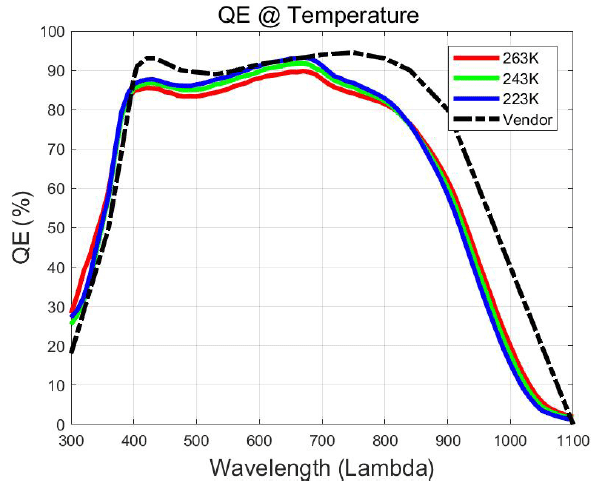
where AD is the active area of the calibrated photodiode in cm2; SCCD is the average output signal of the detector in e-/pix/s; QED is the QE of the photodiode, generally given by the manufacturer; PS is the active area of the detector in cm2; and SD is the signal from the photodiode e-/s. As shown in Eq.(5), QE can be determined by comparing the signal for the detector to that of the calibrated photodiode. Therefore, we measured QE by illuminating the detector using flat field illumination from the monochromator and integrating sphere and measured the absolute light intensity using the calibrated photodiode for comparison at the same location. The measurement was repreated for wavelengths from 300 to 1,100 nm with a step size of 10 nm. Fig. 11 shows the QE measured for the Andor iKon M CCD camera. The maximum QE is 93% ± 2% at 690 nm and 223K.
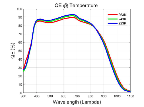
We measured the QE at different temperatures to determine the temperature-dependent properties of the detector. Fig. 11 shows that the QE depends on the temperature. The QE in the visible region increases with decreasing temperature, while the QE in the near-IR region increases with decreasing temperature.
As the temperature decreases, the band gap of silicon increases such that incident photons travel longer and the length of the photon absorption increases (Mcfarlane & Roberts 1955; Braunstein et al. 1958). The backside-illuminated detector, as adopted in the Andor iKon M CCD camera, has a thinner silicon substrate than to the front-illuminated detector. Because near-IR photons can travel longer with decreasing temperature, there is a higher possibility that the photons penetrate the silicon substrate, which leads to a decrease of the QE in the near-IR region. In addition, semiconductors have a dead layer at their surface, which generates additional charges when photons penetrate this layer (Wall et al. 2013). This increases the sensitivity and QE of the backside-illuminated detector, specifically in the visible region. Note that photons have shorter wavelengths, such as UV, that are reflected or absorbed by the surface, which leads to a worse QE, regardless of the temperature. Based on the QE measurement, we conclude that the QE in the visible region varies from 2 % to 5 % and that in the near-IR region varies by 30 % or more depending on the temperature.
4 DISCUSSION AND CONCLUSION
We present KASI′s experimental setup for the dectector performance test and characterize the Andor iKon M CCD camera. We measured the conversion gain, FWC, nonlinearity, dark current, read noise, signal-to-noise ratio, pixel defects, and QE. The measured values are summarized in Table 4.
The conversion gain is a fundamental factor of the detector characteristics. The output signals in ADU generated from accumulated charges vary depending on the electronics configuration such as the user-defined gain setting. Therefore, it is required to convert the output signal to an absolute input reference number, e−. In addition, this relationship is used to measure the different detector characteristics, such as the read noise, dark current, FWC, and QE, and compare the performances of different detectors. We will use another method to measure the gain value for the sanity check in the future (based on a Fe-55 source). It can be simply calculated by dividing the peak of the pixel values in the pixel histogram by 1,620 e−. In addition, as shown in Eq. (1), the conversion gain is a product of different gain components. We will also design an experimental setup for the measurement of individual components.
The measured FWC is 130,000 e-, with a variation of ′1%. Because the FWC provides an observational limitation before pixel saturation, many manufacturers have applied advanced technology to increase the FWC for the same pixel size. Except for the employed technology, it is affected by the silicon substrate voltage, extending the electrical field inside the pixel. Holland (2006) and Simms et al. (2007) showed how much the substrate voltage affects the pixel performances. Therefore, an optimized substrate voltage should be determined in future studies.
The nonlinearity is below 2 % in the range of 10 − 90 % FWC. This reveals that the absolute brightness of an observed star can be reproduced within an uncertainty of 2 %. Therefore, to achieve a better photometry accuracy than 2 %, postprocessing is required to correct for the nonlinearity.
Because the dark current has a strong correlation with the temperature, the precise measurement of the dark current at a given operation temperature is necessary to minimize the uncertainty. We neglected two contributors during the dark current analysis, that is, diffusion and surface dark currents. Diffusion dark currents are generated by balancing between the doping and intrinsic silicon concentration and are dominant at higher operation temperature such as room temperature. Surface dark currents are generated by an incomplete status between silicon substrate and epitaxial region. Both dark currents can be reduced by applying advanced manufacturing technology and are negligible at lower operation temperature. We demonstrated that the generation dark current is the dominant source for the Andor iKon M camera and determined its activation energy.
energy. As shown in Eq. (4), read noise is composed of various components. The results show that the temperature plays an important role in the increment of read noise at higher temperature, typically higher than 273 K. This shows that the dark current components are the most dominant contributors to read noise. The results of Janesick (2007) are consistent with the results of our experiment. However, the read noise variation depending on the temperature is almost negligible at lower temperature, typically lower than 263 K. On the other hand, the source follower noise is known as the dominant noise source at lower temperature (Janesick 2007) and is significantly sensitive to the readout speed. Therefore, if any application requires the change readout speed (high or low) at lower operation temperature, proper measurements of the readout noise are required for both modes.
If the observation requires a bigger pixel size and observed targets are imaged within a few pixels, the detection of pixel defects becomes more important for the development of the data reduction algorithm (Park et al. 2013, 2016). Therefore, the defect pixel locations and an appropriate analysis method need to be defined.
We prove that the QE varies up to several percent in the visible region, while it varies up to tens of percent in the near-IR range. This indicates that the operation temperature plays an important role in the instrumentation performance, specifically in the NIR region. In addition, the measured QE varies depending on the selection of the camera window. A broadband VUV–NIR window is currently used for the Andor iKon M Camera and its transmission efficiency is almost 94 % over the wavelength range from 300 to 1,100 nm.
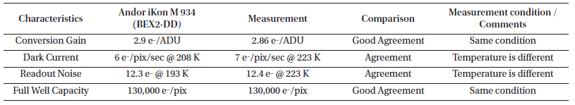
Finally, we compared the results of the measurements with the performance test results provided by the vendor for verification (private communication). As shown in Table 5, our measurements are in good agreement with those from the vendor. Note that the operation temperature for the measurement of the dark current and read noise is different because the vendor evaluated the camera system at a lower temperature using a coolant chiller. This explains the difference between our measurements and that of the vendor. However, the results are consistent with our conclusion that the readout noise is insensitive to the operation temperature at lower temperature.
|
Unlike vendor-measured characteristics (Table 5), the QE values were not provided by the vendor. However, the general QE of the Andor iKon M CCD camera product line was provided (measured at 293 K). Although it is hard to directly compare the QE with ours, it can be used to verify the overall QE performance. Fig. 12 demonstrates that a higher temperature leads to an increase of the QE performance in the near-IR range, which is consistent with our results. However, the maximum QE of the vendor is 95 % at 750 nm, while we obtained 93 % at 690 nm. In addition, the QE values in the visible region are different and the QE of the vendor is a few percentages higher than our value, although the QE from the vendor was measured at higher operation temperature. It is hard to explain the origin of this discrepancy because the measurements were not performed using the same configuration and conditions.
We will continuously evaluate the characteristics of detectors using the newly developed experimental setup (visible to IR detectors such as the H2RG). We will measure the charge transfer efficiency, modulation transfer function, intra-pixel capacitance, and individual pixel sensitivity. The characterization methods and test equipment will be applied to develop the next generation of astronomical instrumentation.